Lessons Learned while Sending my First PCB to Fabrication
I’ve just ordered my first custom home-grown, glacier-watered, grass-fed printed circuit board (4.5 years after graduating with an EE degree, yikes!) and wanted to jot down some notes from the process while everything is still fresh. If you’re getting tired of breadboards and hand soldering but have felt intimidated at the process of jumping into full circuit design without the help of a development board, hopefully you can glean something from this short post and it will inspire you to make the leap!
First off, as I mentioned I do have a degree in electrical engineering and while I’ve never made a PCB myself, I’ve been around many people who have and I suspect I’ve picked up a decent amount by osmosis; it feels a little disingenuous to claim complete 101 level knowledge here. However, all the knowledge I had was “in theory” and there was a lot of missing knowledge on my part that I had to fill in during the process.
For a long-ish, but highly information dense introduction I really can’t recommend enough a video by the YouTube channel Phil’s Lab where Phil walks through a basic design including an STM32 microcontroller, USB, and some other common peripherals. He starts from a blank KiCAD 6.0 project and ends with how to export the correct files to be used by a specific manufacturer, JLCPCB. I watched it in full and then again in pieces several times and it’s what enabled me to get started: KiCad 6 STM32 PCB Design Full Tutorial - Phil’s Lab #65.
Some key pieces of wisdom I picked up for schematics:
- For an STM32-based board, plan out your pin usage with STM32CubeMX.
- Decoupling capacitors: 1 uF + n 100 nF where n is the number of Vdd/Vss pairs (including VddA/VssA).
- Label ALL of your nets (important later for PCB layout).
The video is full of great wisdom and you will probably re-use large chunks of that design for many many STM32 based boards you could envision.
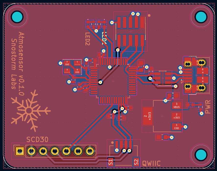
Moving on to the PCB layout, Phil details through some useful best practices and organization, but I lucked out and also received some wisdom from my friend Alex Young who does this stuff for a living:
- After laying out components and edge cuts, make your ground plane for your back copper layer. Find other power nets like
Vbusand make smaller pours for those on your front copper and place your components to take advantage of this efficiently. Then place your 3V3 pour on your top copper layer with a lower priority than your other pours. In KiCAD higher priority is higher number, which is evidently reversed in Altium. - While it’s important to place important signals like USB data early, sometimes you need to sneak a via in that your design rules will make harder to sneak in after. Just do it first so the software can help you.
- Best practice: one
GNDvia per pad that needs it (exception being decoupling capacitor ground pads close to micro pins). - If you feel squished routing traces on one side of your micro, double check that you can’t move some of those signals to another side (STM32CubeMX really helpful here).
When it comes time to get the board manufactured, the video does a pretty good job, but it seems like maybe the end is cut just short of the full process. The files that are generated by KiCAD are also not quite ready to go to JLCPCB specifically. I had to make two modifications:
- For the BOM file, I had to remove the “Collated Components” section. When it came time to pick components JLCPCB was detecting all of my components twice and it was making me unable to proceed. I eventually determined this was the fix.
- For the pick-and-place CSV file, you need to change some headers in the top row. Specifically:
Ref->Designator,PosX->Mid X,PosY->Mid Y,Rot->Rotation, andSide->Layer.
Finally, you pick all of your components that you want populated and it will render a model of your PCB to make sure everything is right. Almost definitely the component orientations are not correct, check literally everything. I had to rotate most of my components to get them to line up pin 1. In one case it had my QWIIC connector translated strangely on the board. I had to click Align in their UI and it snapped into place where it was supposed to be.
After everything looks good, you can submit and pay for the order and hopefully after a couple hours you get a confirmation e-mail from JLCPCB with a graphic like this!
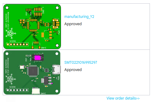
Congrats, your (and currently my) PCB is in fabrication and soon on its way! If my board comes back wonky or messed up, I’ll be sure to come back and edit this post with my findings so that your board does not come back wonky or messed up!
If you notice a dead link or have some other correction to make, feel free to make an issue on GitHub!