Making a PCB Antenna in KiCAD 6.0
I’ve been going back to my hardware roots a little bit lately and trying out electrical and PCB design for a project I’ve been thinking about for a while. There will be two boards talking wirelessly over nRF24L01 transceivers at 2.4 GHz. One of my biggest stumbling blocks during the process has been adding an antenna similar to the one I see on all of the hobby board for this chip. Since I am making my own board and didn’t want to just add pin breakouts to plug in a board I set out to add a PCB antenna.
It turns out it’s shockingly difficult to find information on this (or maybe I don’t know the right keywords). I found some videos going way too deep on the math and skipped those. I knew that somewhere there had to be exact dimensions for the antennas used on all of these cheap hobby boards but I just couldn’t find it. I even considered trying to measure it myself from a board I have. Finally, on the KiCAD Discord somebody pointed me to an application from Texas Instruments: AN043. It has the exact dimensions needed for the antenna!
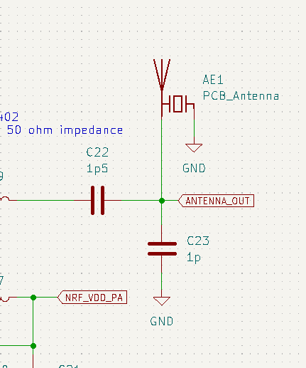
Next, I had to figure out how to add the right symbol in a way that would make the electrical rules checker happy. I ended up selecting the Antenna_Chip symbol which has two pins: one for FEED and the other for GND. I plopped it into my schematic where it looks like this:
Next I had to create the appropriate footprint which is quite a different process from creating footprints for normal parts. The entire antenna needs to be exposed copper and you need a custom shape. Luckily we can refer to the app note for the dimensions.
You’ll need to go into KiCAD’s Footprint Editor. Start with a couple SMD pads for the FEED and GND pads. Once you’ve created them, you need to make sure they’re in the right position relative to one another. If you right click a pad, there’s a menu for Special Tools and under that is Position Relative To.... In the menu box that opens, select the other pad and set the dimensions. Take care to note that you’re setting the dimensions between the centerpoint of each pad, not the edges.
Next on the right hand tool tray you’ll want to make sure you select the Layer F.Cu for front copper and then the Draw a rectangle tool. This part stumped me for an annoyingly long time: to use the tool, you need to single click without dragging. If you drag, it does nothing. You single click, then it will show you a box as you move your pointer. Single click again to place the other corner. Now you’ll need to configure your dimensions exactly as shown in the app note, set the Line Width to 0, and click the Filled Shape checkbox. Add all of the pieces and you are good to go! Save it into whatever footprint library is appropriate!

Finally you need to go back to your schematic and associate the footprint with your schematic symbol. If you double click on your schematic symbol, there should be a menu box with a table. One row has a Name of footprint and you can double click the Value column for that row to select your newly made footprint.
I have only just done this, so we will see if any of the above actually works soon when I lay out the rest of my board and it comes back. If not, I’ll edit the above with my findings.
If you notice a dead link or have some other correction to make, feel free to make an issue on GitHub!